













Quick Answer
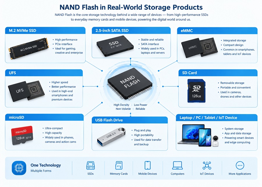
NAND Flash is a type of non-volatile memory that retains stored data even when the device is powered off, until the data is erased or replaced. It is the core storage technology inside Solid State Drives (SSDs), eMMC modules, SD cards, microSD cards, USB flash drives, and mobile devices.
NAND Flash stores data within microscopic memory cells. Based on how many bits of data each cell holds, NAND is categorized into SLC, MLC, TLC, and QLC. The memory cell type has a major influence on a storage drive’s density, cost, write endurance, and performance characteristics.
However, NAND Flash is only one part of a complete SSD. Final real-world speed and lifespan also depend on the SSD controller, custom firmware, interface standards (such as PCIe NVMe or SATA), cache design, and real-world thermal conditions.
What Is NAND Flash?
NAND Flash is a form of non-volatile solid-state memory designed for persistent digital data storage. Unlike volatile system memory (DRAM), which loses all stored information when a system reboots or shuts down, NAND Flash retains data even when power is disconnected, until it is explicitly overwritten or erased.
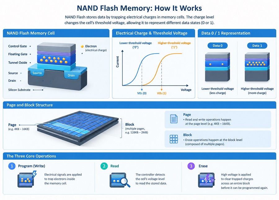
Architecturally, NAND Flash is structured into smaller units called pages and larger structures called blocks:
- Read and write operations take place at the page level (commonly 4KB to 16KB).
- Erase operations take place at the larger block level (composed of multiple pages).
Because new data cannot be written to a cell without erasing the entire block first, NAND Flash requires specialized management techniques to handle data updates efficiently over time.
How Does NAND Flash Work?
NAND Flash memory stores digital information by trapping and holding electrical charges inside individual memory cells. The amount of stored electrical charge affects the cell's threshold voltage, allowing the memory to represent different data states.
The basic operation of NAND Flash consists of three core actions:
- Programming (Writing): Electrical signals are applied to trap electrons inside the memory cell.
- Reading: The controller detects the voltage level of the cell to read the stored binary data.
- Erasing: High voltage is applied to clear trapped charges across an entire memory block before it can be programmed again.
Because memory cells experience gradual physical wear through repeated write and erase actions, storage drives rely on intelligent memory controllers to execute wear leveling, error correction, and background garbage collection. For a deeper breakdown of how the management center handles these operations, see How SSD Controllers Work: The Engineering Behind SSD Performance, Thermal Throttling, and Lifespan.
NAND Flash Types: SLC, MLC, TLC, and QLC
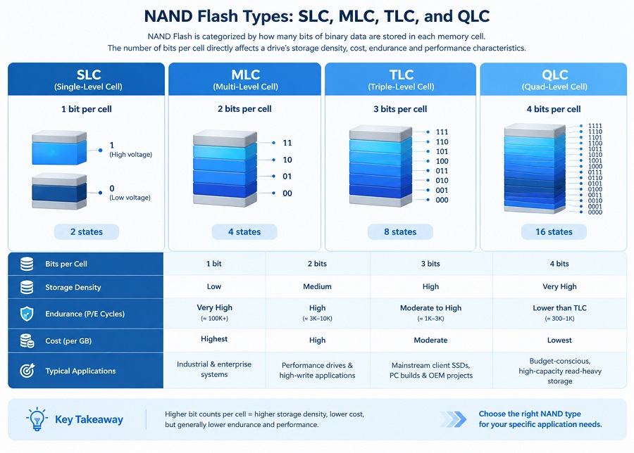
NAND Flash is categorized by how many bits of binary data are packed into each individual memory cell.
| NAND Type | Bits per Cell | Storage Density | Relative Endurance | Typical Positioning |
|---|---|---|---|---|
| SLC (Single-Level Cell) | 1 | Low | Very High | Specialized industrial & enterprise systems |
| MLC (Multi-Level Cell) | 2 | Medium | High | Legacy performance drives & high-write applications |
| TLC (Triple-Level Cell) | 3 | High | Moderate to High | Mainstream client SSDs, PC builds & OEM projects |
| QLC (Quad-Level Cell) | 4 | Very High | Lower than TLC | Budget-conscious, high-capacity read-heavy storage |
SLC NAND
SLC (Single-Level Cell) stores 1 bit of data per cell. Because each cell represents only two electrical states, SLC offers exceptionally fast write performance, extremely low latency, and maximum write endurance. However, its low storage density makes it significantly more expensive per gigabyte, limiting its use primarily to specialized industrial and enterprise systems.
MLC NAND
MLC (Multi-Level Cell) stores 2 bits per cell across four electrical states. MLC provides higher capacity density than SLC while maintaining relatively high write endurance. While widely used in earlier performance SSDs, modern multi-layer 3D TLC has largely replaced traditional MLC in mainstream markets.
TLC NAND
TLC (Triple-Level Cell) stores 3 bits per cell across eight electrical states. TLC is widely used in mainstream consumer SSDs, laptop upgrades, and client PC integration because it offers a practical balance of capacity, performance, endurance, and cost.
For a comprehensive breakdown of how TLC compares directly against QLC in real-world workloads, see TLC vs QLC SSD: Performance, Endurance, Lifespan, and Which NAND Is Better?.
QLC NAND
QLC (Quad-Level Cell) stores 4 bits per cell using 16 distinct electrical states. Storing more bits per cell maximizes storage capacity and reduces the cost per gigabyte. The trade-off is generally lower native write endurance and slower write speeds when writing large files continuously, making it best suited for budget-conscious or read-heavy applications.
Does NAND Flash Have a Fixed Speed?
NAND Flash components do not have a single fixed speed rating. The sequential and random speeds published on an SSD box are the result of several system components working together.
Real-world flash performance depends on factors such as:
- NAND Generation & Layers: Newer 3D NAND with higher layer counts can improve storage density and may contribute to higher overall performance when combined with an appropriate controller and architecture.
- Multi-Channel Parallelism: SSD controllers read and write across multiple NAND dies simultaneously to multiply throughput.
- Bus Interface: Physical interface bandwidth limits, such as PCIe 4.0 x4, PCIe 3.0 x4, or SATA III.
- Controller Architecture & Firmware: Algorithms regulating data traffic and background maintenance.
- Operating Temperatures: Thermal throttling algorithms that temporarily slow down speeds to prevent hardware overheating during heavy tasks.
What Is SLC Cache and How Does It Affect Performance?
Many modern TLC and QLC SSDs use an SLC Cache to deliver high peak write performance during everyday tasks.
In an SLC cache design, a portion of the TLC or QLC NAND is dynamically configured to behave like fast SLC memory (storing only 1 bit per cell temporarily). This allows incoming files to be saved rapidly for short bursts, improving system responsiveness during:
- Launching games or heavy creative applications
- Transferring moderate-sized files
- System booting and routine software updates
Sustained Write Performance
Because the SLC cache buffer is finite, continuously writing large volumes of data (such as transferring massive raw video files) can eventually exhaust the cache. When this happens, write speeds may drop to the NAND’s native TLC or QLC write speed as the drive writes directly to native cells.
How Does NAND Flash Affect SSD Endurance (TBW)?
NAND Flash cells can only withstand a limited number of write and erase cycles before their ability to hold a reliable charge degrades.
SSD lifespan is commonly measured in TBW (Terabytes Written), which estimates the total volume of data that can be written to the drive over its lifetime under normal operating conditions. To understand how manufacturers calculate these limits and how they relate to everyday drive usage, read SSD TBW Explained: What It Means and How It Affects SSD Lifespan.
While the cell architecture (SLC, TLC, or QLC) sets the baseline for endurance, actual real-world SSD longevity is also influenced by:
- Quality Screening: High-grade NAND dies display better voltage stability and fewer inherent errors.
- Controller Management: Efficient wear-leveling algorithms prevent specific memory blocks from wearing out prematurely.
- Over-Provisioning: Allocating additional hidden flash capacity enables the controller to swap out degraded blocks seamlessly over time.
NAND Flash vs. DRAM: What Is the Difference?
NAND Flash and DRAM serve fundamentally different purposes inside modern computing architectures:
| Feature | NAND Flash | DRAM |
|---|---|---|
| Data Retention | Non-volatile (Retains data when powered off) | Volatile (Loses data instantly without power) |
| Primary Role | Long-term file, OS, and software storage | High-speed temporary working memory for the CPU |
| Speed | Fast (Microseconds latency) | Extremely Fast (Nanoseconds latency) |
| Use in SSDs | Primary persistent storage medium | Optional high-speed buffer for address translation |
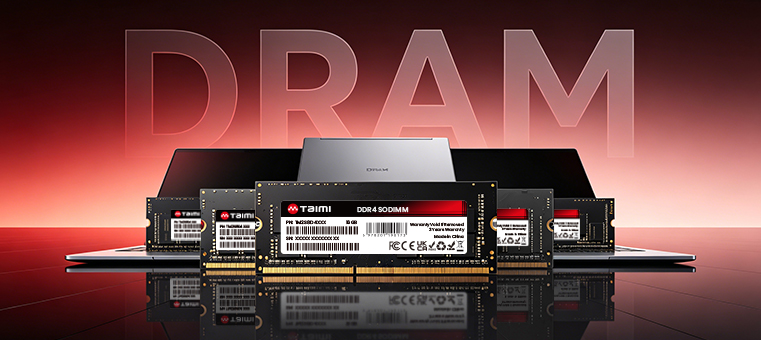
NAND Flash handles persistent storage, while DRAM provides temporary high-speed data access. Some entry-level SSDs feature a "DRAM-less" design, using host system RAM via PCIe protocols (Host Memory Buffer) to maintain cost efficiency while preserving high performance.
NAND Flash vs. Finished SSD: Are They the Same?
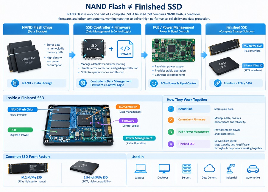
No. NAND Flash is a memory technology, while an SSD is a complete, standalone storage device.
An SSD contains several essential components:
- NAND Flash Memory: The physical silicon chips that store raw data.
- SSD Controller: The onboard processor that manages host communication, wear leveling, and data distribution.
- Firmware: The operating software embedded inside the controller.
- Circuit Board & Interface Connection: The physical PCB, power management ICs, and interface connectors (M.2 NVMe or 2.5-inch SATA).
Where Is NAND Flash Used?
- Client & OEM SSDs: Used in desktops, laptops, all-in-one PCs, and gaming handhelds via M.2 PCIe NVMe and 2.5-inch SATA form factors.
- Embedded Storage: Integrated solutions like eMMC and UFS used in compact devices, tablets, and smart home electronics.
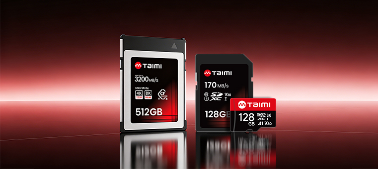
- Removable Storage: SD cards, microSD cards, and USB drives for cameras, smartphones, and portable media storage.
What Should Buyers Consider When Choosing Storage?
When evaluating NAND-based storage for personal PC upgrades, system builds, or OEM procurement, look beyond basic peak sequential speed numbers. Consider:
- Capacity & Application: Match drive capacity and NAND type (TLC vs. QLC) to your intended workload (e.g., primary OS boot drive vs. secondary media backup).
- Interface Compatibility: Ensure your motherboard supports the corresponding protocol (PCIe 4.0, PCIe 3.0, or SATA III).
- Endurance & Warranty: Check the TBW rating and manufacturer warranty terms to ensure long-term reliability for your usage volume.
- Manufacturing Quality & Consistency: For bulk procurement and OEM projects, verified batch consistency and production testing are critical to long-term deployment stability.
Final Takeaway
NAND Flash is the core non-volatile technology behind modern digital storage. While cell types like SLC, MLC, TLC, and QLC explain fundamental differences in storage density and theoretical endurance, an SSD's real-world behavior is determined by how NAND Flash works together with its controller, firmware, interface, and thermal management.
Looking for Reliable SSD Solutions for Your OEM Projects?
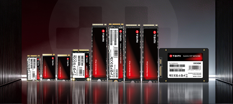
Taimi (苔米) is a specialized storage manufacturer offering a comprehensive portfolio of PCIe 4.0, PCIe 3.0, and SATA III SSDs backed by full-process SMT production control and a 3-year warranty.
Contact Taimi to Request Free Samples & Spec SheetsFrequently Asked Questions (FAQ)
1. What is NAND Flash used for?
NAND Flash is used for non-volatile digital data storage in SSDs, eMMC/UFS embedded storage, SD cards, microSD cards, and USB flash drives.
2. Is TLC or QLC NAND better for an SSD?
Neither is universally better. TLC generally offers stronger sustained write performance and higher endurance, making it ideal for primary OS drives and intensive gaming. QLC provides higher storage density at a lower cost per gigabyte, making it suitable for high-capacity, read-heavy media storage.
3. Does NAND Flash determine overall SSD speed?
NAND Flash heavily influences baseline speed, but it does not determine SSD performance alone. The SSD controller, firmware, channel architecture, interface protocol, and SLC cache design all contribute significantly to final real-world speeds.
4. Is NAND Flash faster than DRAM?
No. DRAM is significantly faster than NAND Flash with lower latency. However, DRAM is volatile memory and loses data without continuous power, whereas NAND Flash provides persistent long-term storage.
5. What is the difference between NAND Flash and an SSD?
NAND Flash is the raw memory technology used to hold data charges, while an SSD is a complete storage device that integrates NAND Flash chips with a controller, firmware, circuit board, and host interface.